Scalable Nanoimprint Manufacturing of Achromatic Metalenses from a High-Refractive-Index, Low-Shrinkage Photoresist
GA, UNITED STATES, September 22, 2026 /EINPresswire.com/ -- Chinese researchers developed a onestep nanoimprint
Press Release Disclaimer: This is a press release distributed through the XPR Media network. It has not been independently verified by our newsroom.
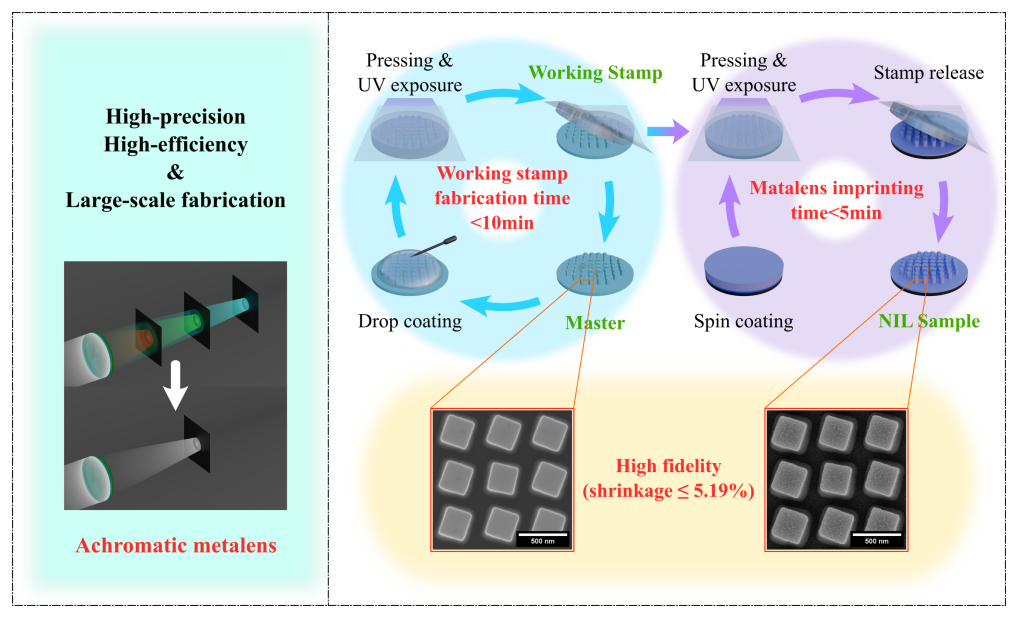

GA, UNITED STATES, September 22, 2026 /EINPresswire.com/ — Chinese researchers developed a onestep nanoimprint lithography process for achromatic metalenses (480–640 nm) using a novel photoresist with high refractive index (1.92–1.97), high transmittance (>99%), and low shrinkage (≤5.19%). The working stamp is cured in minutes. The fabricated metalens exhibits excellent focusing and achromatic performance, with focallength deviation <2% across the bandwidth.
Optical metalenses – ultrathin arrays of subwavelength nanostructures – promise to miniaturise imaging systems, but chromatic aberration and the lack of scalable, lowcost fabrication methods have hindered their practical adoption. Conventional electronbeam lithography offers high resolution but suffers from low throughput, while deepultraviolet lithography involves high equipment costs and complex multistep processes. Nanoimprint lithography (NIL) is a promising alternative, yet existing imprint resists often exhibit excessive shrinkage (up to ~20 %) after curing, compromising structural fidelity and optical performance.
In a paper published in Light: Advanced Manufacturing, a research team led by Professors Nan Zhang (Beijing Institute of Technology) and Wanjiao Zhang (University of Chinese Academy of Sciences) reports a scalable NIL route for achromatic metalenses operating across the 480–640 nm band.
The researchers highlight three key contributions of their novel manufacturing approach:
(1) Development of a highrefractiveindex, lowshrinkage photoresist – The team formulated a hybrid photoresist based on an acrylate polymer matrix, incorporating TiO₂ nanoparticles to boost the refractive index, together with silane and methacrylfunctionalised silane as shrinkage inhibitors. These inhibitors strengthen interfacial bonding between the inorganic phase and polymer matrix and tailor the crosslinking network structure. They restrain the movement of polymer segments and facilitate stress release during curing, effectively limiting both lateral and vertical shrinkage to ≤5.19 %. Optical characterisation showed that the resist achieves a refractive index of 1.92–1.97 and transmittance >99 % over the wavelength range of 480–640 nm, with TiO₂ nanoparticles uniformly dispersed (average particle size ~26 nm), well below the minimum feature size, ensuring complete filling during imprinting.
(2) Fast UVcurable working stamp and highefficiency imprint process – Traditional NIL often relies on thermally cured polydimethylsiloxane (PDMS) stamps, which require several hours of curing. In contrast, this work uses a novel UVcurable resin that fully cures in just 3 minutes under a 300 W UV lamp. Combined with an automated imprinter, the entire workingstamp fabrication is completed within 10 minutes. Subsequently, using this stamp on a glass substrate spincoated with the photoresist, the imprinting, exposure, and demoulding steps are finished in another 5 minutes. Thus, the whole process – from stamp to final metalens – can be accomplished in 15 minutes, and the stamp is reusable, providing a solid foundation for lowcost mass production.
(3) Highfidelity fabrication and validated achromatic performance – To quantify manufacturing accuracy, the team systematically measured the dimensions of nanopillars in the master, working stamp, and final imprinted samples using SEM and FIBSEM. Statistical results show that the average shrinkage rates for width, length, and height were only 2.23 %, 1.87 %, and 3.47 %, respectively, with maximum shrinkage not exceeding 5.19 %. This confirms nearperfect structural replication. Benefiting from this high precision, the fabricated metalens was optically tested across 480–640 nm. The measured focal lengths remained highly consistent at different wavelengths, with a maximum deviation <2 %. The focal spot size was close to the diffraction limit. Simulations corrected by introducing the measured dimensional deviations are still in good agreement with experimental data, indicating that the proposed high‑refractive‑index nanoimprint material and metalens fabrication strategy enable precise dimensional control of meta‑atom structures and satisfy the stringent high‑precision fabrication requirements for achromatic metalenses.
“This work provides a practical route for the highprecision, highefficiency, and largescale production of achromatic metalenses,” the team concludes. “The demonstrated photoresist and fastcuring stamp materials have substantial application potential in compact imaging, augmented reality displays, and integrated photonics.”
DOI
10.37188/lam.2026.105
Original Source URL
https://doi.org/10.37188/lam.2026.105
Funding information
This work was supported by the National Natural Science Foundation of China (Grant No. 62575023).
Lucy Wang
BioDesign Research
email us here
Legal Disclaimer:
EIN Presswire provides this news content “as is” without warranty of any kind. We do not accept any responsibility or liability
for the accuracy, content, images, videos, licenses, completeness, legality, or reliability of the information contained in this
article. If you have any complaints or copyright issues related to this article, kindly contact the author above.

Media gallery